
The rapid and unrelenting evolution of artificial intelligence has fundamentally altered the trajectory of global computing infrastructure. As massive language models and generative artificial intelligence clusters grow exponentially larger, the sheer volume of data moving through data centers has completely shattered previous networking paradigms. Historically, the architectural bottleneck of high-performance computing lay within the processor itself; today, the limitation is no longer how fast a chip can calculate, but rather how fast data can be fed into and extracted from that chip. As AI clusters expand to encompass tens of thousands of individual accelerators, they have traditionally relied upon optical interconnects exclusively for scale-out connectivity—linking multiple distant server racks across sprawling data center floors. However, the physical constraints of traditional electrical signaling mean that the day when systems require optical interconnects for intricate, short-reach scale-up connectivity is rapidly approaching.
To proactively prepare for this inevitable paradigm shift, a historic coalition of the world’s most powerful technology companies has been forged. Hyperscalers Microsoft, Meta, and OpenAI—the entities currently purchasing the vast majority of the world’s AI compute—have formally teamed up with legendary hardware designers AMD, Broadcom, and Nvidia. Together, this unprecedented consortium has established the Optical Compute Interconnect (OCI) Multi-Source Agreement (MSA) group. Their shared mission is singular yet monumental: to collaboratively develop a completely protocol-agnostic, open optical connectivity specification specifically designed for scale-up interconnections within massive AI systems and racks. This initiative effectively signals the beginning of the end for traditional copper cabling in high-performance AI routing, paving the way for a future where light replaces electricity as the primary medium for localized, high-speed data transfer.
The Escalating Demands of Generative AI
The transition from classical machine learning to deep generative AI has necessitated a complete rethinking of datacenter architecture. The parameters of state-of-the-art models now number in the trillions, requiring a computational framework that can act as a single, unified supercomputer rather than a collection of isolated servers.
To support these massive workloads, data center engineers must overcome several distinct hardware limitations. The following architectural elements are currently undergoing rapid, forced evolution to prevent systemic bottlenecks.
- The memory bandwidth capacity of individual graphics processing units (GPUs).
- The latency limitations inherent in traditional top-of-rack switching topologies.
- The thermal management required to cool intensely dense computational nodes.
- The physical spatial constraints of routing thousands of thick electrical cables.
The Limitations of Traditional Scale-Up Connectivity
In the context of AI data centers, “scale-out” refers to connecting multiple separate computing nodes across a network, while “scale-up” refers to connecting multiple processors within a single node or adjacent racks so they function as one massive accelerator. Until now, scale-up domains have relied heavily on copper-based electrical interconnects. However, as signaling speeds increase to keep pace with newer generations of AI accelerators, copper cables suffer from severe signal degradation and physics-based limitations. The faster the electrical signal travels, the shorter the copper cable must be to maintain data integrity, eventually restricting the physical size and layout of AI compute racks. This physical boundary is precisely why the transition to optical scale-up interconnects is no longer a theoretical luxury, but an absolute engineering necessity.
The Formation of the OCI Multi-Source Agreement
The establishment of the Optical Compute Interconnect (OCI) MSA represents a deeply strategic realignment of the global semiconductor and networking industries. In a landscape historically characterized by fierce proprietary competition, the unification of these specific tech titans underscores the existential importance of solving the optical networking bottleneck.
An Unprecedented Alliance of Tech Titans
The founding membership of the OCI MSA reads like a directory of the most influential entities in the modern technology sector. On the demand side, you have Microsoft, Meta, and OpenAI, hyperscalers that are currently deploying billions of dollars in capital expenditure to build the most advanced AI infrastructures on the planet. On the supply side, you have AMD, Broadcom, and Nvidia, the undisputed titans of semiconductor design and networking hardware. The fact that Nvidia and AMD—two fierce rivals locked in a battle for AI accelerator supremacy—are collaborating within the same agreement highlights the universal necessity of a common optical standard. By agreeing to standardize the physical optical layer, these companies ensure that their respective proprietary protocols can operate efficiently without forcing hyperscalers into restrictive, vendor-locked physical infrastructure silos.
This unprecedented level of industry cooperation is designed to streamline the adoption of next-generation hardware. The consortium aims to eliminate several major friction points that currently plague datacenter architects.
- The high costs associated with designing custom networking solutions for different chipsets.
- The severe interoperability issues between competing hardware ecosystems.
- The prolonged development cycles required to test proprietary communication protocols.
- The massive supply chain risks associated with single-vendor physical layer dependencies.
Hyperscaler-Driven Over Vendor-Driven
One of the most defining characteristics of the OCI MSA is its unique organizational power dynamic. While traditional industry groups are often spearheaded by independent hardware vendors (IHVs) attempting to push their specific intellectual property onto the broader market, the OCI MSA is fundamentally hyperscaler-driven. Microsoft, Meta, and OpenAI are dictating their exact operational requirements, power constraints, and deployment timelines directly to the hardware manufacturers. This top-down approach ensures that the resulting optical connectivity specifications are perfectly tailored to the rigorous, real-world demands of massive-scale AI training and inference facilities. It shifts the focus from theoretical hardware capabilities to practical, deployable datacenter solutions that prioritize predictable power consumption and seamless integration at scale.
The Technological Foundation of OCI
To truly appreciate the impact of the Optical Compute Interconnect, one must delve into the deeply sophisticated technological foundation that the MSA is building. The group is not merely designing a new cable; they are actively defining the future physical laws of localized data transmission within supercomputing environments.
Understanding the Common Optical Physical Layer (PHY)
At the core of the OCI specification is the development of a common optical physical layer, universally referred to as the PHY. In networking architecture, the PHY is the foundational layer responsible for the actual transmission and reception of unstructured raw data bits over a physical medium. By establishing a unified optical PHY, the OCI MSA guarantees that regardless of the specific higher-level protocols being utilized, the foundational mechanism for shooting lasers across a glass fiber remains entirely standardized. This practice means the consortium is effectively commoditizing the optical hardware layer, allowing hyperscalers to drastically reduce costs by utilizing unified components, standard optical transceivers, and universal fiber cabling infrastructure across their entire fleet of heterogeneous AI accelerators.
The standardization of the physical layer introduces a multitude of engineering efficiencies for hyperscale data centers. These specific operational benefits are crucial for maintaining the rapid pace of AI cluster deployment.
- Simplified inventory management through the use of interchangeable optical components.
- Reduced training requirements for datacenter technicians deploying the hardware.
- Streamlined diagnostic procedures when troubleshooting physical connection failures.
- Enhanced scalability by allowing phased upgrades of individual compute nodes.
Protocol Agnosticism: Unifying UALink and NVLink
Perhaps the most commercially significant aspect of the OCI MSA is its strict commitment to protocol agnosticism. In the highly competitive world of AI accelerators, the communication protocols that dictate how GPUs talk to one another are heavily guarded proprietary assets. Nvidia relies on its incredibly dominant NVLink technology, while a competing coalition led by AMD and Broadcom recently introduced the Ultra Accelerator Link (UALink). The genius of the OCI specification is that it does not attempt to replace these protocols; rather, it provides a universal, high-speed optical highway upon which both NVLink and UALink traffic can seamlessly travel. This allows hyperscalers to mix and match different processors and switches from competing suppliers over the exact same fiber infrastructure, retaining maximum flexibility while hardware developers maintain their distinct competitive advantages at the protocol level.
Breaking Down the Optical Mechanics: NRZ and WDM
The actual transmission of data over the OCI standard relies on cutting-edge optical engineering principles. The MSA has specifically chosen highly robust, proven methodologies to ensure data integrity at unprecedented speeds, explicitly selecting NRZ signaling and WDM technology as the bedrock of their optical roadmap.
The Mechanics of NRZ Signaling
The OCI connectivity technology for short-reach optical links will initially define its common PHY based on Non-Return-to-Zero (NRZ) signaling. In the realm of digital communications, NRZ is a binary code where ones and zeros are represented by distinct, constant voltage or light levels, without returning to a neutral zero state between bits. While some broader networking standards have transitioned to more complex modulation schemes like PAM4 (Pulse Amplitude Modulation with 4 levels) to cram more data into a single signal, the OCI’s choice of NRZ for short-reach scale-up links is highly deliberate. NRZ signaling offers incredibly low latency and requires significantly less power for signal processing and error correction compared to PAM4. In the tightly constrained thermal and latency environments of an AI compute rack, the raw, unadulterated speed and simplicity of NRZ signaling make it the optimal choice for connecting adjacent high-performance accelerators.
The deployment of NRZ signaling in this specific architectural context yields several immediate physical advantages. Engineers prioritize these distinct traits when designing tightly packed compute clusters.
- Significantly lower bit error rates before the application of forward error correction.
- Reduced power consumption at the transceiver level due to simpler digital signal processing.
- Decreased end-to-end latency, which is hyper-critical for synchronous AI model training.
- Easier integration with existing electrical SerDes (Serializer/Deserializer) architectures.
Wavelength-Division Multiplexing (WDM)
To achieve the massive bandwidth required by next-generation AI, the OCI specification heavily leverages Wavelength-Division Multiplexing (WDM). WDM is a technology that multiplexes a number of optical carrier signals onto a single optical fiber by using entirely different wavelengths—essentially different colors—of laser light. This means that multiple, independent streams of data can travel simultaneously down the exact same microscopic strand of glass without interfering with one another. The OCI roadmap dictates a starting point of four distinct wavelengths, each operating at 50 Gigabits per second (Gb/s), yielding a combined throughput of 200 Gb/s per direction. By utilizing WDM, the OCI standard maximizes the data-carrying capacity of the physical fiber infrastructure, allowing for massive future scalability simply by adding more “colors” of light to the transmission without needing to lay thicker, heavier bundles of cables.
Advancing Hardware: From Pluggables to Co-Packaged Optics
The OCI specification is explicitly designed to be forward-looking, accommodating the rapid physical evolution of optical networking hardware. As data speeds increase, the physical distance between the silicon chip and the optical laser must shrink to prevent electrical signal loss, leading to a massive shift in how optics are packaged and deployed.
The Role of Pluggable Optical Modules
In the initial phases of the OCI rollout, the technology will heavily support traditional pluggable optical modules. These are the familiar, hot-swappable transceivers that plug into the front faceplates of network switches and specialized compute nodes. Pluggables offer incredible flexibility, allowing datacenter operators to easily upgrade, replace, or repair optical links without taking the entire server offline. Furthermore, they allow hyperscalers to source transceivers from a wide variety of third-party vendors, driving down costs through fierce market competition. However, as AI scale-up interconnects push toward the terabit-per-second threshold, the electrical traces required to route the signal from the ASIC (Application-Specific Integrated Circuit) processor deep inside the server to the pluggable module on the front panel become a massive source of power consumption and signal degradation.
To mitigate the limitations of front-panel pluggables, the industry is rapidly developing alternative hardware form factors. The OCI standard explicitly accommodates these emerging packaging technologies to ensure future viability.
- On-board optics (OBO) which move the optical transceivers off the faceplate and directly onto the motherboard.
- Liquid-cooled optical assemblies designed to manage the intense heat generated by high-speed lasers.
- Highly dense fiber ribbon connectors capable of routing hundreds of optical channels simultaneously.
- Advanced retimer chips that actively condition the electrical signal before it reaches the optical engine.
Direct ASIC Integration and Co-Packaged Optics (CPO)
To truly unlock the extreme bandwidths required later in the decade, the OCI MSA is heavily focused on supporting Co-Packaged Optics (CPO). Co-packaging involves completely eliminating the traditional standalone transceiver and integrating the optical silicon directly onto the same underlying substrate as the compute processor or network switch ASIC. By moving the conversion point of electricity to light mere millimeters away from the processing core, CPO drastically reduces the electrical transmission distance. This results in incredibly massive reductions in power consumption and allows for a density of optical I/O (Input/Output) that is physically impossible with traditional pluggable modules. As Near Margalit, Vice President & General Manager of the Optical Systems Division at Broadcom, emphasized, the OCI-MSA allows for “seamless integration with existing electrical SerDes-based ASICs while providing a clear path to direct ASIC integration, ensuring the ecosystem remains flexible and high-performing.”
The Strategic Vision of the Founding Members
The creation of the OCI MSA is not merely an engineering endeavor; it is a highly strategic business maneuver by the world’s leading technology firms. Examining the public statements of the founding members reveals a unified vision for the future of global computing infrastructure.
AMD and Broadcom’s Commitment to Open Standards
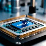
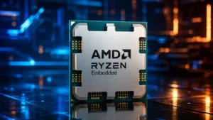
For companies like AMD and Broadcom, the OCI MSA represents a critical opportunity to level the playing field against highly vertically integrated competitors. Brian Amick, Senior Vice President of Technology & Engineering at AMD, clearly articulated this vision, stating, “The growing need for optical scale-up interconnect to support large AI systems later this decade is clear. AMD is a founding member and strong supporter of the OCI MSA as it establishes an open specification for the industry to foster a robust, multi-vendor optical scale-up interconnect ecosystem.” By aggressively pushing for an open standard, AMD ensures that its deeply impressive lineup of MI-series AI accelerators can be seamlessly integrated into any hyperscaler’s optical network. Broadcom, a pioneer in CPO technology and advanced networking silicon, similarly benefits from an open ecosystem that allows its industry-leading optical components to be adopted across a wide variety of competing compute platforms.
The pursuit of open standards provides significant strategic leverage against proprietary networking monopolies. These companies utilize open consortiums to achieve specific long-term business objectives.
- Accelerating the global adoption of their proprietary compute silicon by removing networking friction.
- Fostering a broad ecosystem of third-party component manufacturers to rapidly drive down hardware costs.
- Aligning deeply with the procurement philosophies of hyperscalers who despise vendor lock-in.
- Pooling highly expensive research and development resources to solve fundamental physics challenges.
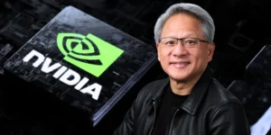
Nvidia’s Quest for Super-Intelligence Infrastructure
Nvidia’s participation as a founding member is arguably the most fascinating dynamic within the OCI MSA. As the undisputed king of AI hardware, possessing a massive market share and its own highly successful proprietary NVLink ecosystem, Nvidia technically had the most to lose by joining an open physical standard. However, Nvidia recognizes that the absolute scale required for the next generation of artificial general intelligence (AGI) transcends the physical manufacturing capabilities of any single company. Gilad Shainer, Senior Vice President of Networking at Nvidia, noted, “By equipping best-in-class compute with state-of-the-art optics, the OCI MSA can deliver the scale and performance required by the next era of super-intelligence.” Nvidia understands that standardizing the underlying optical glass does not threaten their dominance; rather, it rapidly accelerates the build-out of massive AI clusters, ultimately allowing them to sell vastly more GPUs to hyperscalers who are no longer bottlenecked by copper cabling constraints.
The Speed of Innovation: Why an MSA?
In the highly bureaucratic world of technology standardization, the specific legal and organizational structure chosen by these companies is deeply telling. The decision to form a Multi-Source Agreement (MSA) rather than funneling the technology through a traditional standards body is a massive indicator of the extreme urgency surrounding AI infrastructure development.
Bypassing Traditional Standard Bodies
While the OCI MSA group is headed by organizations known for supporting open industry standards, it is explicitly not a traditional standard-setting body like the JEDEC Solid State Technology Association or the recently formed Ultra Ethernet Consortium (UEC). Traditional standards bodies are designed to unite tens or even hundreds of competing companies across an entire global industry. This massive inclusivity fundamentally requires lengthy, deeply bureaucratic consensus processes, exhaustive peer reviews, and painfully slow voting mechanisms. In the hyper-accelerated era of generative AI, waiting three to five years for a traditional standards body to ratify a new physical layer specification is absolutely commercially unacceptable. The technology would be hopelessly obsolete before the first draft was officially published.
The MSA framework provides a rapid alternative to bureaucratic stagnation. This agile organizational structure is specifically utilized when time-to-market is the primary objective.
- Allows a highly select, deeply focused group of deeply aligned companies to finalize specifications rapidly.
- Bypasses the necessity for broad, industry-wide consensus on highly specific architectural details.
- Enables immediate prototyping and interoperability testing between the founding partner organizations.
- Facilitates the rapid commercial deployment of cutting-edge hardware to meet immediate hyperscaler demand.
Rapid Deployment for the Super-Intelligence Era
By utilizing the MSA structure, the OCI group—at least in its initial phases—enables AMD, Broadcom, and Nvidia to aggressively build interoperable short-reach interconnections specifically tailored for Microsoft, Meta, and OpenAI at unprecedented speeds. Because it targets a very specific architectural layer of AI systems (short-reach links within a scale-up domain) rather than attempting to standardize a vertically integrated set of technologies for the broader enterprise market, the scope of the agreement is incredibly tight and actionable. This massive reduction in development friction is precisely what is meant to simplify system integration, radically reduce development risk, and drastically shorten deployment cycles for new, highly advanced generations of AI hardware.
The OCI Technology Roadmap: From 200 Gb/s to 3.2 Tb/s
The Optical Compute Interconnect specification is not a static document; it is a highly dynamic, aggressive technological roadmap explicitly designed to scale alongside the insatiable bandwidth demands of future AI models. The founding members have laid out a clear, phased approach to achieving unprecedented data transmission rates over the next decade.
Phased Scaling Strategies
The initial iteration of the OCI specification establishes a highly robust, immediately achievable baseline utilizing deeply proven optical technologies. As previously noted, the standard starts at four individual wavelengths operating at 50 Gb/s using NRZ signaling, achieving 200 Gb/s per direction. However, this is merely the foundational stepping stone. Over time, the aggressive roadmap is fully expected to massively expand both the total wavelength counts (packing more colors of light into the fiber) and the underlying signaling rates of those individual wavelengths. The consortium is explicitly targeting scaling the physical layer all the way to 800 Gb/s per individual fiber in the near term.
The path to multi-terabit optical connectivity requires overcoming several highly complex physical barriers. The roadmap explicitly targets these critical engineering milestones for future development.
- Transitioning to more advanced, higher-density WDM grids to support eight or sixteen distinct wavelengths.
- Implementing highly sophisticated error correction algorithms that do not introduce unacceptable latency penalties.
- Developing highly resilient silicon photonics manufacturing processes to dramatically increase production yields.
- Optimizing the thermal dissipation capabilities of Co-Packaged Optics to manage massively increased laser power.
Future-Proofing Global AI Infrastructures
The ultimate stated goal of the OCI roadmap is to push the bandwidth boundaries to a staggering 3.2 Terabits per second (Tb/s) per fiber, and potentially beyond, as the broader optical ecosystem naturally evolves. By clearly defining this long-term trajectory, the MSA provides massive, deeply necessary assurance to the hyperscalers investing billions of dollars in new physical data centers. Microsoft, Meta, and OpenAI can confidently pour concrete and lay dark fiber infrastructure today, knowing with absolute certainty that the optical physical layer specification will support the massive throughput required by the AI processors of 2030 and beyond. This unified, highly predictable roadmap is the absolute bedrock upon which the next era of global super-intelligence will be constructed.
Conclusion
The establishment of the Optical Compute Interconnect (OCI) Multi-Source Agreement is a deeply monumental milestone in the history of computer engineering. As artificial intelligence models rapidly transcend the physical computational limits of single processors, the ability to seamlessly connect thousands of accelerators into massive, unified super-clusters has become the ultimate determinant of technological supremacy. By decisively recognizing that traditional copper interconnects have finally hit an impenetrable physical wall, the coalition of Microsoft, Meta, OpenAI, AMD, Broadcom, and Nvidia has proactively ensured that the explosive growth of AI will not be bottlenecked by outdated physical infrastructure.
Through the rapid, hyperscaler-driven development of an open, protocol-agnostic optical physical layer, the OCI MSA is fundamentally physically rewiring the data center. Whether accommodating the proprietary brilliance of Nvidia’s NVLink or the open-ecosystem power of AMD and Broadcom’s UALink, the OCI specification provides the highly versatile, massively scalable optical highway required to transport the immense datasets of tomorrow. As the roadmap rapidly scales from 200 Gb/s to an astonishing 3.2 Tb/s per fiber, the transition from electrical to optical scale-up interconnects will unlock unprecedented levels of computational power. Ultimately, the work being done by the OCI consortium today is the critical, silent enabler of the artificial general intelligence breakthroughs of tomorrow, guaranteeing that the physical hardware of the future can effortlessly support the limitless ambitions of software developers worldwide.