
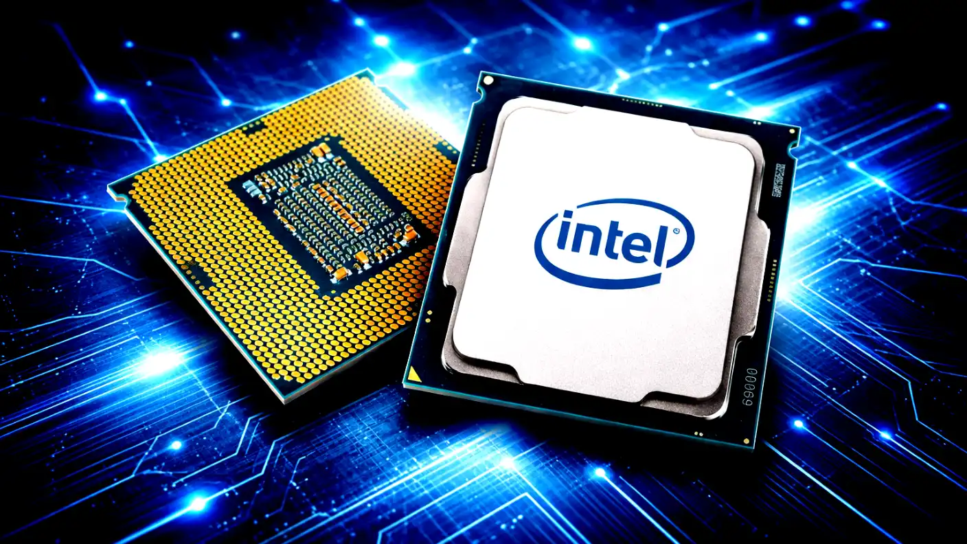
Intel is doubling down on its aggressive foundry strategy, aiming to reclaim the crown in semiconductor manufacturing. The company recently unveiled details regarding its upcoming 14A Gen2 node, a high-stakes technological leap designed to put significant distance between Intel and rivals like TSMC and Samsung. By integrating dual-side power delivery technology, Intel believes it can offer superior performance and efficiency, effectively changing the rules of the game for chip production.
The core of this innovation lies in how the chips manage electricity. Traditionally, power and data signals compete for space on the front side of a silicon wafer. Intel’s new dual-side approach clears that bottleneck by separating these functions, placing power delivery on the back of the chip. This shift allows for a 15% increase in transistor density and a massive jump in performance-per-watt. For customers designing next-generation AI processors, these gains are not just incremental; they are transformational.
This move comes at a vital moment for the company. Intel has committed over $100 billion to expanding its global manufacturing footprint, with the 14A Gen2 node serving as the flagship technology for these new facilities. As competition in the AI chip sector hits a fever pitch, Intel needs to prove that its “five nodes in four years” roadmap is not just a marketing slogan but a concrete reality. Success with the 14A process would provide the company with a major advantage over TSMC, which is currently the dominant player in the foundry market.
Engineers at Intel are already calling the 14A Gen2 node a “generational leap.” By optimizing the power delivery network, they have managed to reduce voltage drop by nearly 20%, which directly translates to cooler chips and longer battery life for mobile devices. These improvements are critical for data centers as well, where even a 1% improvement in energy efficiency can save millions of dollars in annual electricity costs for companies operating thousands of server racks.
However, the path forward is not without challenges. Samsung has been making its own strides with gate-all-around (GAA) transistor technology, and TSMC continues to refine its N2 process with extreme precision. Intel must execute its transition to the 14A Gen2 node with flawless reliability. The company is investing roughly $30 billion in new extreme ultraviolet (EUV) lithography tools to ensure it has the capacity to produce these advanced chips at a commercial scale, rather than just in a lab setting.
The foundry business requires extreme consistency, and Intel knows it. By providing transparent performance metrics and early access to design kits, the company is attempting to woo back the massive fabless chip designers who moved their business to TSMC during Intel’s previous manufacturing slumps. If Intel can deliver on its promise to bring 14A Gen2 to mass production by 2027, it could capture a significant slice of the lucrative high-end AI processor market.
Looking at the broader economic picture, the battle for supremacy in 14-nanometer-class technology is about more than just profit. It is about national security and technological sovereignty. With trillions of dollars in global commerce depending on the availability of advanced semiconductors, Intel’s ability to manufacture these chips domestically is a major talking point for policymakers. The company is currently on track to receive over $8 billion in government support under the CHIPS Act, funds which are earmarked specifically for advancing these high-end manufacturing capabilities.
As Intel prepares for the rollout of the 14A Gen2 node, the tech world will be watching closely. Whether the company can successfully out-engineer TSMC and Samsung remains the million-dollar question. If the performance claims hold up, Intel may finally have the firepower to reclaim its position as the undisputed leader in silicon manufacturing. For now, the hardware industry remains in a state of high anticipation, waiting to see if these engineering breakthroughs can reshape the future of computing.