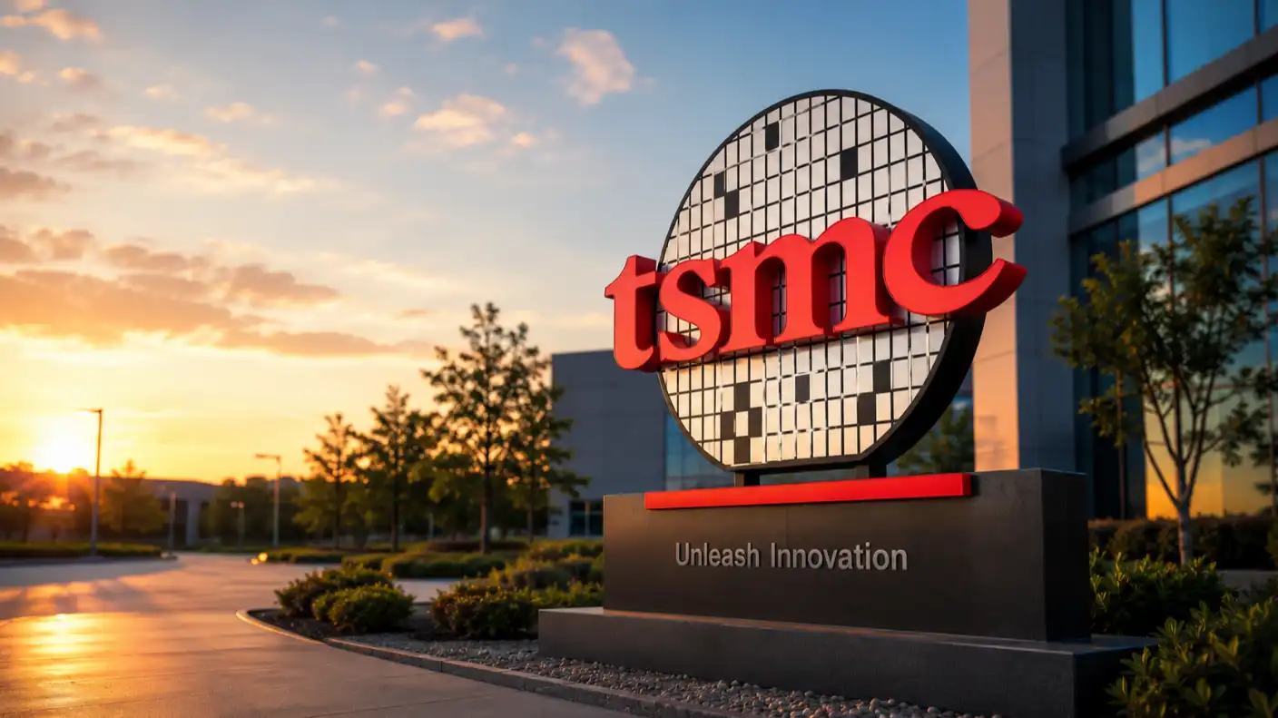
The race to power the next generation of artificial intelligence is hitting a physical limit. As AI processors grow larger and demand more energy, traditional organic substrates are starting to struggle with heat and data transmission. To solve this, TSMC is heavily investing in a groundbreaking shift: replacing conventional materials with glass substrates. This move promises to keep the company at the forefront of the CoWoS (Chip-on-Wafer-on-Substrate) packaging ecosystem while unlocking performance levels that silicon and organic materials simply cannot match.
Engineers have long known that glass offers superior thermal stability compared to current organic alternatives. During intense operations, chips expand and contract, which can cause micro-cracks in traditional substrates. Glass, however, maintains its shape with much higher precision. Because glass mimics the thermal expansion properties of silicon more closely than organic materials, it significantly reduces the risk of mechanical failure. This allows TSMC to pack more transistors into a smaller space without worrying about the structure warping under high temperatures.
One of the most exciting advantages of glass is its ability to support higher-density interconnects. AI chips require massive amounts of bandwidth to move data between the processor and high-speed memory. Glass substrates act as a superior foundation for these intricate pathways, allowing for a 50% improvement in connection density. With these tighter interconnects, data travels faster and with less electrical resistance. This change translates directly into shorter latency times and a more responsive experience for users running complex models like ChatGPT or advanced real-time simulations.
Despite these clear performance benefits, TSMC is taking a calculated, patient approach to mass production. The manufacturing process for glass substrates is still vastly different from the established methods used for organic substrates. Moving from a flexible, plastic-like base to a rigid, brittle material requires entirely new assembly lines. Estimates suggest that mass production will not reach scale until at least 2027 or 2028. Currently, the company focuses on perfecting the yield rates, as even a 1% failure rate in the advanced packaging stage can cost millions of dollars in wasted high-end silicon.
The cost factor also looms large over the transition. While the performance gains are massive, producing glass substrates currently costs 20% to 30% more than the legacy organic counterparts. TSMC remains in the prototyping phase, working closely with equipment suppliers to refine the laser-drilling and bonding techniques required for this new material. By perfecting these steps now, the firm aims to drive down costs before it rolls the technology out for the general market.
Industry analysts view this as a necessary evolution rather than a luxury. Modern GPU clusters in data centers already consume upwards of 1,000 watts per card, and keeping these systems cool while maintaining data integrity is the primary hurdle for hardware designers. If TSMC succeeds in perfecting glass packaging, it will effectively remove one of the biggest bottlenecks in computing. By shifting the foundation of the chip itself, they are ensuring that the AI revolution does not stall due to the limitations of traditional packaging materials.
Ultimately, this move solidifies TSMC’s dominant position in the global semiconductor supply chain. By proactively solving the packaging challenges of 2030 today, they maintain their lead over competitors who are still struggling with organic substrate limitations. While consumers may not see glass-based chips on store shelves this year, the foundation for a much faster, cooler, and more efficient AI era is being laid right now in the cleanrooms of TSMC.